
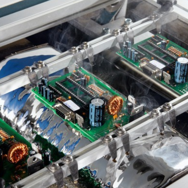
DIP PCBA
-
Heart’s DIP process is a dual-in-line package component mounting process, which is a process that combines traditional electronic components and PCB. Modern new electronic products have emphasized lightness, thinness and short size, so most DIP parts have been SMD Replaced by parts.
The assembly and soldering method of DIP is different from the SMT process. In short, it is manually inserting the parts into the through holes (PTH) of the PCB, using a Flux sprayer to apply an appropriate amount of flux on the bottom of the PCB, and then preheating and soaking in the tin furnace In the tinning process, tin water adheres to the part feet and the PCB through holes, and the electronic parts are combined with the PCB-PAD to complete the assembly and soldering technology, referred to as DIP process. Heart electronic has two DIP production lines of plug-in, repair, hand soldering line and lead-free soldering furnace, and is equipped with constant temperature soldering iron and dispenser. The maximum PCB size can be L400mm*W400mm.
